Photo Gallery

In this image CdTe quantum dots of sizes varying from 3-5 nm emit a range of emission wavelengths through the visible region. The particles are called "quantum dots" because they are a direct example of the "quantum confinement effect" when materials are smaller than the Bohr exciton radius.
More information on quantum confinement can be found Particle In A Box
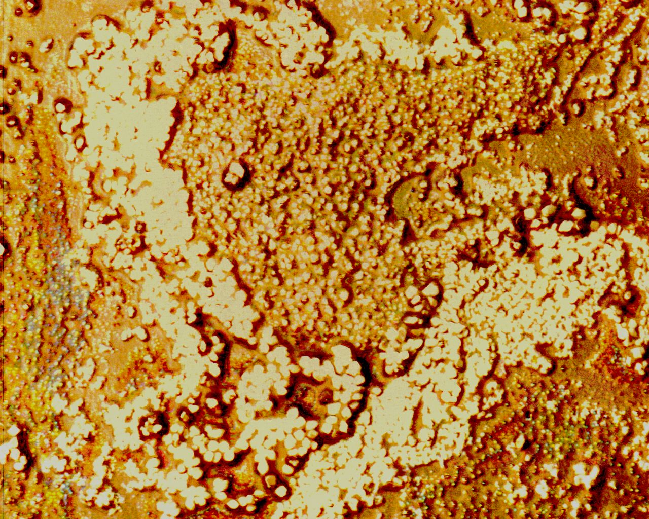
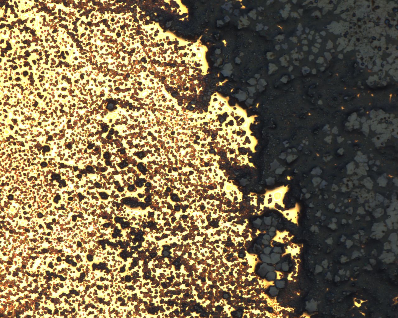
The above images are of a thin film of 5 nm quantum dots on a Si wafers and imaged with the Zeiss CSM 700. While individual QDs are too small to resolve the reflected image gives the impression that we have individual point sources and gives the images a pixelated appearance.
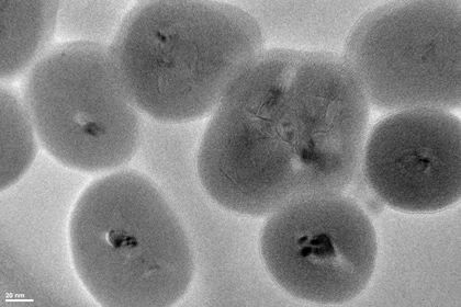
HRTEM image of HPHT NDs with 30 nm SiO2 shells decorated with various functional groups for biosensing and biolabeling applications. The nandiamond hosts the nitrogen vacancy center, a unique atomic defect that is both a magnetic and electric fields sensor. This is possible because of the electron read-out capabilities and the charge switching capabilities of the NV center.The scale bar is 20 nm.
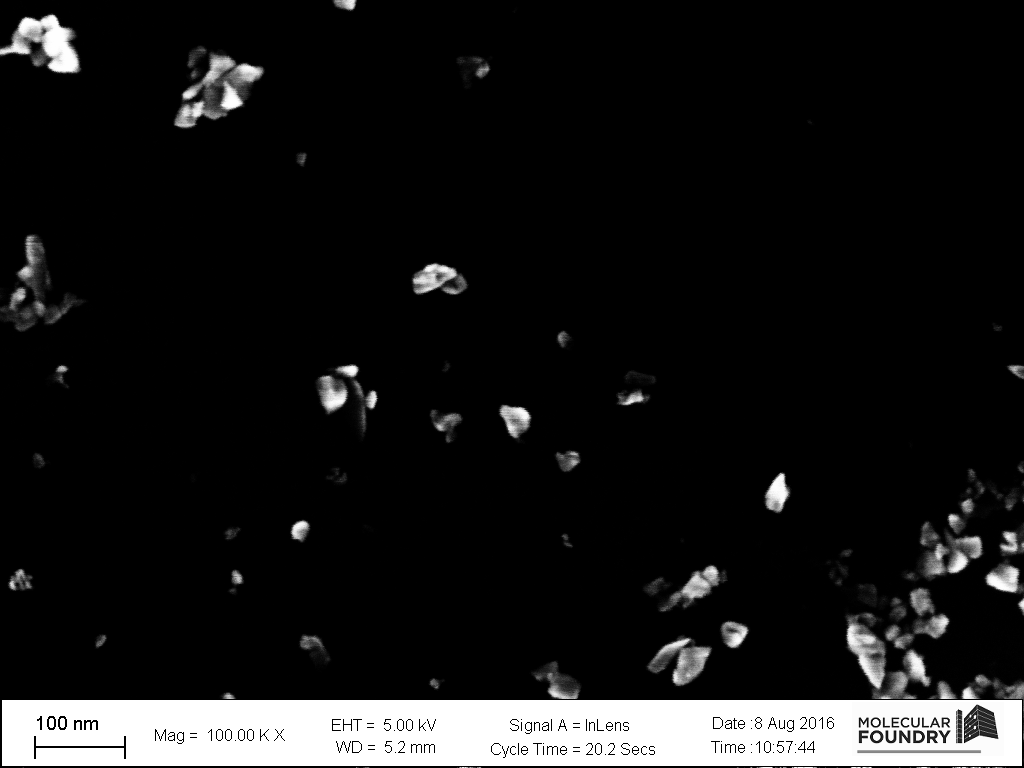
SEM image of unfunctionalized HPHT nanodiamonds. Notice the irregular shape of the nanocrystals. They are formed by the ballmilling of macroscopic single crystal HPHT diamond. Scale bar is 100 nm.
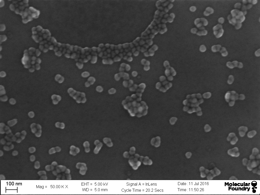
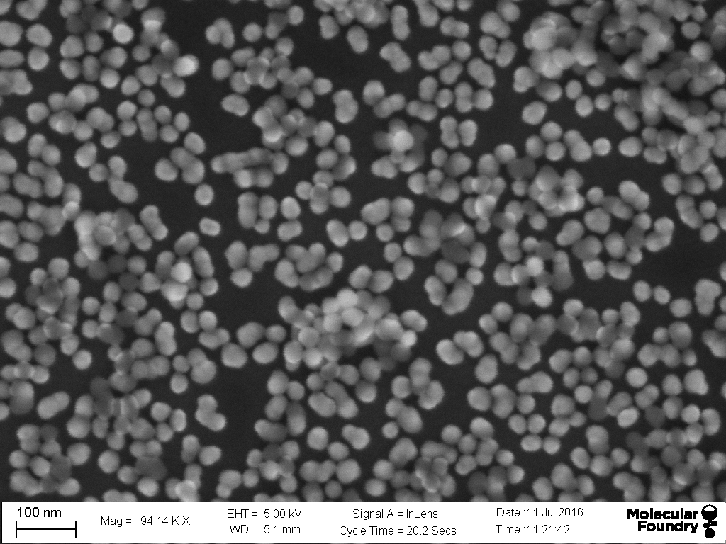
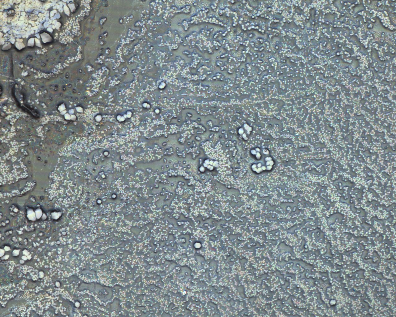
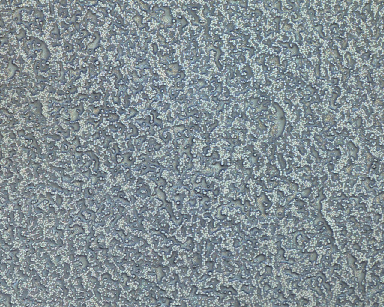
SEM images of 50 nm SiO2 nanoparticles that can be an inexpensive testbed for SiO2 based diamond chemistry and plasmonics. Sclare bar is 100 nm.